Most solar power is produced by converting sunlight into electricity through the use of thin films made of semiconductor materials that absorb particles of light, called photons. These absorbed photons knock electrons loose from atoms in the thin film, and the free electrons are then channeled into an electrical current.
However, even the most popular semiconductor materials, such as crystalline silicon, have limits on how much electrical current they can produce—because the electrons don’t stay free for very long before they recombine with atoms in the film. The materials also need to be highly stable to withstand the heat, humidity, and other environmental conditions found in solar power applications.
In recent years, an inorganic cesium-lead-bromide (CsPbBr3) crystalline perovskite material has shown excellent stability and electron transport capabilities, even in harsh humid environments. A better understanding of the dynamics inside cesium-lead-bromide could help scientists optimize the optical and thermal properties of a wide range of perovskite materials, some of which have demonstrated more than a 25 percent power conversion efficiency, rivaling that of silicon-based materials.
Researchers from Duke University, Northwestern University, and Argonne National Laboratory conducted neutron scattering experiments at the Department of Energy’s (DOE’s) Oak Ridge National Laboratory (ORNL) and have reported the most direct observations to date of the atomic motions inside cesium-lead-bromide crystals. The results were published in Nature Materials in a paper titled, “Two-dimensional overdamped fluctuations of soft perovskite lattice in CsPbBr3.”
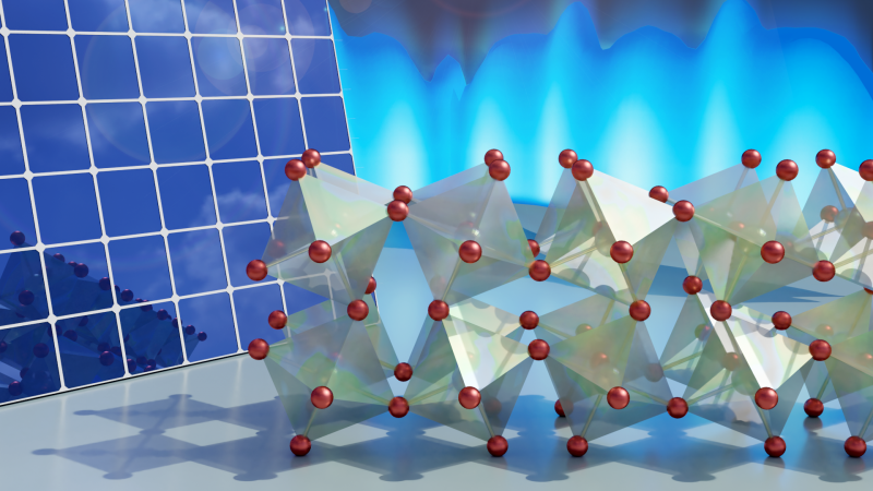
“Our experiments reveal the high power conversion efficiency of cesium-lead-bromide is due in large part to its bromine atoms, which act as “hinges” that enable the rest of the atomic structure to flex and twist,” said Olivier Delaire, associate professor in the Mechanical Engineering and Materials Science Department at Duke University. “This twisting motion is thought to inhibit some free electrons from recombining with the semiconductor atoms, leaving more electrons available to produce an electrical current.”
The researchers started by carefully growing a large, centimeter-scale, single crystal of the perovskite. Despite having the simplest perovskite structure, cesium-lead-bromide crystals are notoriously difficult to grow to such a size, which is one reason why previous studies of the material’s atomic dynamics were not able to achieve the same level of detail.
Another key to the research was using the cold neutron chopper spectrometer (CNCS) and wide angular-range chopper spectrometer (ARCS) instruments at ORNL’s Spallation Neutron Source (SNS). Thanks to their high intensity neutron beams and comprehensive sets of detectors, these two neutron instruments provided the high-resolution data needed to fully illuminate the atomic vibrations characteristic of perovskite materials.
“CNCS and ARCS are the world’s best tools to see and map the periodicity of neutrons scattered from crystal samples,” said Delaire. “Along with complementary x-ray diffraction experiments conducted at Argonne, neutron spectrometry at the SNS allowed us to determine that the data was indeed recording the flexing and twisting of octahedral groupings of atoms.”
Complementary neutron spectrometry was performed at the National Institute of Standards and Technology Center for Neutron Research.
After comparing the neutron and x-ray data with their computer simulations, the researchers confirmed just how active the perovskite’s crystalline structure is. Each 8-sided octahedral group of atoms (imagine two pyramids stuck together back-to-back) is connected to its neighbors by a bromine atom “hinge.” This hinge-like arrangement allows the atomic structure to constantly bend back and forth in a fluid manner.
Scientists have known about the pivot points and that they are essential to a perovskite’s properties, yet the structural dynamics had not been clearly observed.
The fluidity or flexing of the perovskite’s atomic structure is thought to slow down and disrupt the movement of the free electrons, similar to how running in a straight line across a trampoline is more difficult than running across a hard surface. The free electrons can’t get back very quickly to the vacancies created when they were knocked loose by photons, so the electrons are easier to assemble into an electrical current.
The perovskite’s relatively weak atomic bonds also result in a “soft” metal semiconductor material that is easier to make into thin films.
According to Delaire, “Our findings very likely extend to much more complicated perovskites, which many scientists throughout the world are currently researching. As they screen enormous computational databases, the atomic dynamics we’ve uncovered could help them decide which perovskites to pursue.”
Delaire acknowledged the key roles played by his PhD graduate researchers, Tyson Lanigan-Atkins and Xing He, who worked to grow the crystals, develop the computer models, and conduct the experiments. The research was supported by DOE’s Office of Science.
SNS is a DOE Office of Science user facility. ORNL is managed by UT-Battelle LLC for DOE’s Office of Science, the single largest supporter of basic research in the physical sciences in the United States. DOE’s Office of Science is working to address some of the most pressing challenges of our time. For more information, visit energy.gov/science. – by Paul Boisvert


